In the world of electronics, PCB and PCBA are two fundamental terms you’ll encounter constantly. While they sound similar and are visually related, they represent distinctly different stages in the creation of any electronic device. For engineers, procurement specialists, and innovators bringing a product to life, understanding this difference is crucial for effective communication, planning, and sourcing.
This guide will dissect PCB and PCBA from every angle, providing a clear, detailed comparison to help you make informed decisions for your next project.
1. Introduction: The Core of Every Electronic Device
Every smart device around you, from a simple toy to a complex medical instrument, has a heart that makes it function. That heart is built upon a Printed Circuit Board Assembly (PCBA), which itself starts as a Printed Circuit Board (PCB). The confusion between the two is common, but mistaking one for the other can lead to significant delays and cost overruns in product development.
This article serves as your definitive resource, breaking down the differences in definition, composition, manufacturing, and application. By the end, you’ll know exactly what you need at each stage of your product journey and how partnering with a full-service PCBA provider like Yuxun Electronics can streamline your path from concept to market-ready product.
2. Basic Definitions: PCB vs. PCBA
What is a PCB (Printed Circuit Board)?
A PCB is the physical, bare foundation of an electronic circuit. It is a flat, non-conductive substrate (usually fiberglass like FR-4) laminated with thin layers of conductive copper tracks, pads, and vias. These copper features are etched onto the board to create specific pathways for electrical signals, following a pre-designed layout. A finished PCB has no electronic components attached to it—it’s essentially a sophisticated “road map” made of insulating and conductive materials, ready for traffic (electrical current) to flow once the “vehicles” (components) are in place.
In short: A PCB is an unpopulated, non-functional bare board.
What is a PCBA (Printed Circuit Board Assembly)?
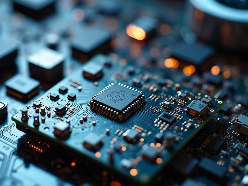
A PCBA is the next evolutionary step. It refers to a PCB that has completed the assembly process and has all the necessary electronic components (resistors, capacitors, integrated circuits, connectors, etc.) soldered onto it. This assembly process transforms the passive “road map” into an active, functional electronic module capable of performing its designated task—whether it’s processing data, amplifying a signal, or controlling a device.
In short: A PCBA is a populated, fully functional circuit board assembly.
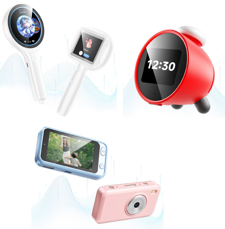
This is where companies like Yuxun Electronics excel. As a National High-Tech Enterprise founded in 2008, we specialize in transforming conceptual designs into high-performance, manufacturable PCBA modules. We provide end-to-end solutions that bridge the gap between a bare PCB and a reliable, intelligent electronic core for products, particularly in the cutting-edge smart toy and AIoT sectors.
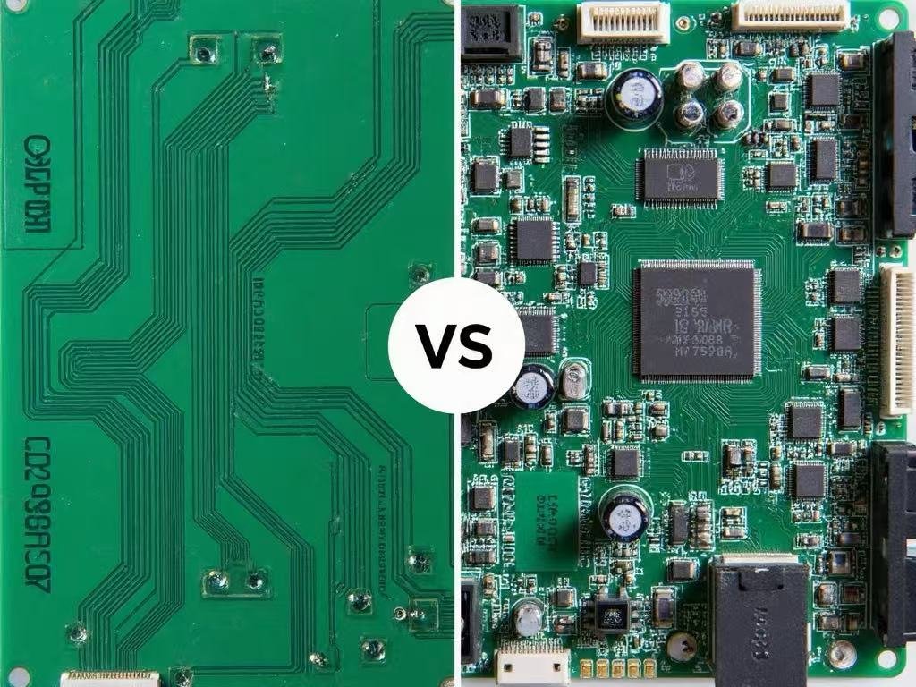
3. Physical Form & Appearance: A Visual Comparison
The most straightforward way to tell them apart is by looking at them.
| Feature | PCB (Bare Board) | PCBA (Assembled Board) |
|---|---|---|
| Components | None. The board is empty. | Populated. Covered with various components. |
| Surface | Shows visible copper traces, solder pads, and a smooth solder mask (often green). | Components and their solder joints cover much of the PCB layout. |
| Functionality | Cannot power on or perform any electronic function. | Can be powered and tested for its intended electronic function. |
4. Materials: What Goes Into Each(PCB&PCBA)?
PCB Materials
- Substrate/Laminate: The insulating core. FR-4 (glass-reinforced epoxy) is most common. Others include flexible materials (Polyimide for flex PCBs), high-frequency materials (Rogers, PTFE), or metal cores (for MCPCBs).
- Conductive Layer: Thin foil of copper, laminated to the substrate. Can be single-sided, double-sided, or multi-layered.
- Solder Mask: The iconic green (or other colors) polymer layer that insulates copper traces and prevents solder bridges.
- Silkscreen: White (usually) ink used for labels, component designators, and logos.
- Surface Finish: Applied to exposed copper pads to prevent oxidation and ensure solderability. Examples: HASL, ENIG, Immersion Silver, OSP.
PCBA Materials
A PCBA incorporates all the materials of the PCB, plus:
- Electronic Components: The active and passive devices (ICs, resistors, capacitors, connectors, sensors, etc.).
- Solder: The metallic alloy (typically tin-lead or lead-free like SAC305) that creates electrical and mechanical bonds. Used as solder paste for SMT or solder wire for hand assembly.
- Additional Materials: Potting compounds for protection, thermal interface materials (grease, pads) for heat dissipation, adhesives for component fixing.
5. Product Characteristics & Nature
| Aspect | PCB | PCBA |
|---|---|---|
| Nature | A component or semi-finished product. It is a part purchased for further assembly. | A functional module or finished product (at the board level). It is the core of an end product. |
| Technical Value | Value lies in design complexity (number of layers, impedance control) and manufacturing precision (fine traces, small vias). | Value is a combination of PCB design, component selection, assembly precision, and firmware/software. It is highly value-added. |
| Focus | Signal integrity, power integrity, thermal management, and mechanical structure. | Overall functionality, performance, reliability, and testability. It’s where hardware meets software. |
For instance, the AI-powered smart toys developed by Yuxun Electronics are not just about advanced PCB layouts; they involve the seamless integration of sophisticated PCBA hardware with intelligent firmware, creating an engaging user experience.
6. The Manufacturing Process: From Blueprint to Board
PCB Fabrication Process:
This is a subtractive and pattern-forming process.
- Design & Output: CAD files (Gerber, drill files) are sent to the fab house.
- Imaging & Etching: The copper-clad laminate is coated with photoresist, exposed to UV light through a film of the circuit pattern, and developed. Unwanted copper is then etched away.
- Lamination & Drilling: For multi-layer boards, layers are aligned and fused under heat and pressure. Holes for vias and through-hole components are drilled.
- Plating & Coating: Holes are plated with copper to connect layers. A solder mask is applied, and a surface finish (e.g., ENIG) is added to pads.
- Testing & Routing: Electrical test (flying probe or fixture test) for continuity and isolation. Boards are routed out from the production panel.
- Final Inspection: Visual and dimensional checks.
PCBA Assembly Process:
This is an additive and assembly process, heavily reliant on automation.
- Solder Paste Application: Solder paste is precisely printed onto PCB pads using a stencil.
- Solder Paste Inspection (SPI): A 3D laser scanner checks the paste volume, area, and height for defects.
- Component Placement (SMT): High-speed pick-and-place machines accurately position surface-mount components onto the pasted pads.
- Reflow Soldering: The board passes through a reflow oven where controlled heating melts the solder paste, forming permanent joints.
- Automated Optical Inspection (AOI): Cameras inspect the board for missing, misaligned, or bridged components.
- Through-Hole Insertion (if needed): Plated-through-hole components are inserted, manually or automatically.
- Wave Soldering (for THT): The board passes over a wave of molten solder to solder the through-hole leads.
- Cleaning, Testing, & Final Inspection: Boards are cleaned (if needed). They undergo rigorous ICT, FCT, and programming (see next section). Final Quality Control checks packaging.
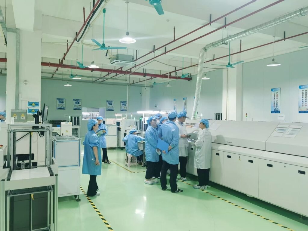
Manufacturing Insight: A robust PCBA partner like Yuxun Electronics owns and controls this critical process. With 3 SMT lines, over 20 automatic testing machines, and a 3,000 sqm modern facility, we have built an integrated smart manufacturing system that ensures quality, consistency, and scalability for volumes up to 500,000 PCBA sets annually.
7. Testing: Ensuring Quality and Function
PCB Testing
- Purpose: Verify the physical and electrical integrity of the bare board.
- Primary Method: Electrical Test. Uses a “Flying Probe” tester or a dedicated test fixture to check for opens (breaks in a circuit) and shorts (unintended connections) against the netlist. It ensures the manufactured board matches the design.
PCBA Testing
- Purpose: Verify the assembly quality, component functionality, and overall performance of the final module.
- Common Methods:
- In-Circuit Test (ICT): Uses a bed-of-nails fixture to access test points. Checks for correct component value, orientation, and basic functionality. Catches assembly defects.
- Functional Test (FCT): Simulates the real operating environment. Powers up the PCBA and validates its full functionality against the product specification. This is where firmware runs and performance is measured.
- Boundary Scan (JTAG): Tests interconnects and functionality of complex ICs.
- Burn-in/Environmental Stress Screening (ESS): Subjects boards to elevated temperature and voltage to identify early-life failures.
- Software/ Firmware Download: Programming the final software into memory chips.
8. How Are PCB and PCBA Related?
Think of their relationship as a sequential and dependent evolution:
- Stage Progression: The PCB is the essential first stage; the PCBA is the completed, functional outcome. You cannot have a PCBA without a PCB.
- Design Interdependence: PCBA design rules (DFM/DFA – Design for Manufacturing/Assembly) heavily dictate PCB layout constraints (component spacing, pad size, via placement). A good PCB design is one that can be efficiently and reliably assembled into a PCBA.
- Supply Chain Integration: PCBA manufacturing is the nexus point that integrates three major supply chains: PCB fabrication, component sourcing, and assembly services. Managing these separately is complex and risky.
9. The Core Differences: Summary Table
| Dimension of Comparison | PCB (Printed Circuit Board) | PCBA (Printed Circuit Board Assembly) |
|---|---|---|
| Definition | Bare, unpopulated board providing mechanical support and electrical connections. | Fully assembled board with all components soldered on, forming a functional circuit. |
| State | Semi-finished product. | Finished product (at board level). |
| Composition | Laminate, copper, solder mask, silkscreen. | PCB + Electronic Components + Solder. |
| Primary Function | Provides electrical connectivity pathways. | Performs a specific electronic function. |
| Manufacturing Focus | Fabrication (etching, lamination, drilling). | Assembly (placement, soldering, testing). |
| Testing Focus | Connectivity (opens/shorts). | Functionality, performance, reliability. |
| Value Proposition | Material and precision fabrication value. | Integrated design, component, assembly, and intellectual property value. |
10. How to Choose for Your Project: PCB or PCBA Service?
- You might only need PCBs if: You are a large OEM with in-house component sourcing and assembly departments, or you are responsible for the final system integration yourself.
- You need a Full-PCBA Service Partner like Yuxun Electronics if:
- You want to focus on your core idea and market strategy, not manage complex supply chains (PCB fab, component vendors, assembly house).
- Your product involves advanced electronics, high-reliability requirements, or a fast time-to-market.
- You need complete, turnkey solutions—from concept design and hardware/software co-development to prototyping and mass production.
- Your goal is to shorten development cycles, reduce total cost of ownership, and guarantee量产质量. Our track record shows we help clients shorten R&D cycles by an average of 15%.
11. Our PCBA Services: Your End-to-End Innovation Partner
At Yuxun Electronics Technology Co., Ltd., we are more than just a manufacturer; we are your innovation partner on the journey from a spark of an idea to a successful product in the hands of users.
- End-to-End Expertise: We offer a seamless, one-stop service covering Concept & Design → Hardware/Software Co-Development → PCB Layout → Component Sourcing & Management → Precision Manufacturing (SMT) → Comprehensive Testing → Scalable Mass Production.
- Proven Technical Capability: As a National High-Tech Enterprise with over 20 years of collective process expertise and a 50-person R&D team (60% technical staff), we hold 30+ patents and software copyrights. We excel in AI-integrated smart products.
- Reliable Quality & Scale: Our in-house, vertically controlled manufacturing system, certified processes, and 98%+ customer satisfaction rate from serving 2000+ global clients ensure you receive dependable, high-quality PCBAs.
- Collaborative Success: We have successfully executed over 10 technology transfer projects for research institutes, proving our ability to transform advanced concepts into manufacturable, market-ready products.
Ready to bring your electronic product vision to life with precision and reliability? Contact Yuxun Electronics today for a free consultation or project review. Let’s discuss how our comprehensive PCBA solutions can accelerate your path to market and give you a competitive edge.